One of the most common things we do with IoT and hardware devices is to dump the firmware that is being used to control the devices.
If we’re lucky, this can be grabbed from an external SPI flash. There are many many articles, bits of hardware, and processes to achieve this.
So what if the firmware is embedded in an MCU on the device? Most microcontrollers have some form of embedded storage in place.
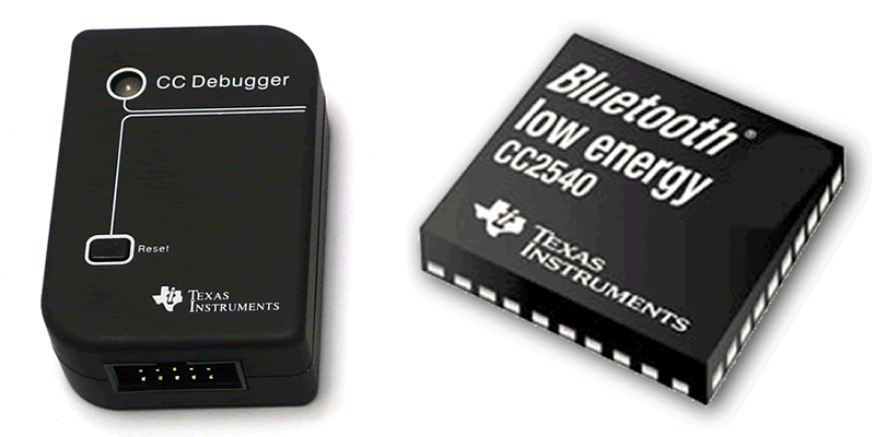
I had this recently on a test, where the device used a Texas Instruments CC2540 MCU to manage its Bluetooth and USB functionality. This is a commonly used chip that we’ve seen before on disparate products, such as the August smart lock and the Master smart padlock so, fortunately we’ve had some experience.
How to start
We will be using a Texas Instruments CC-Debugger, bought for around £50 from a popular electronics retailer. The debugging side of the chip is well documented by Texas Instruments in the CC-Debugger user guide.
For reading Flash data, the debugger needs at least five pins:
- GND (To provide a refence to ground)
- Vdd (To provide a reference to positive voltage)
- RESETn (To set the MCU into debug mode)
- DD (Debug Data, to transfer data)
- DC (Debug Clock, to set the clock for the data stream)
There are also SPI pins for sniffing packets, but we’re not interested in them.
Searching through the user guide shows that we need to connect the points to the legs for RESETn, P2.2 and P2.1. The pinout can be found in the datasheet.
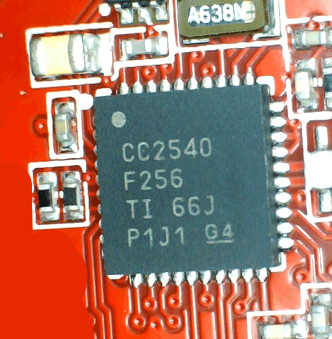
The chip itself is tiny, being 6mm by 6mm; as you can see below, by comparing it to the size of nearby SMD resistors and capacitors. This means that we can’t just hook grippers to correct legs of the chip.
Fortunately every board I’ve seen that uses a CC2540 (or close relative) seems to have a selection of test pads that can be used for in-circuit programming, such as below:
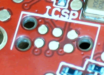
These are six pads (remember we only need five) with holes that are designed to hold a test probe in place, which uses something like pogo pins to make an electrical connection.
To prove these are the correct connectors we need to make sure that they’re connected to the CC2540. This can be performed using a multimeter in continuity mode to buzz out the pads.
There’s one slight problem here though, GND and Vdd can be found quite quickly, but all the other pins have a capacitor between the test pad and the chip leg- making it hard to get a simple connectivity test.
Unfortunately, the only way to go through this is to trace the connections by hand and buzz out between different components. I ultimately had to guess at DC on this board as I could work it out. This was made a lot harder as the test pads were on the other side of the board to the CC2540.
In the end I had the connections, which were hacked together in a spreadsheet (which is how I normally do this):
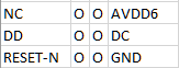
Where the top is towards the double holes in the above screenshot. NC here means Not Connected.
Getting Ready
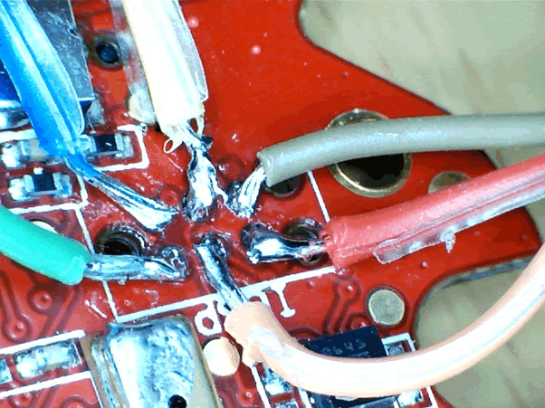
As I didn’t have a connector to fit the pin out and pitch above, what I had to do was to solder a wire to each pad. Now my soldering had improved through practice since my last blogged attempt, but this was hard! Each pad was less than a millimetre in diameter and I couldn’t make it to the office to use a finer pitched soldering iron head and thinner wire.
I spent about thirty minutes cutting wires, stripping wires, tinning pads, tinning wires and delicately soldering oversized wires to small pads with the wrong sized tools for the job. If you want to do stuff like this, get a magnifying headset with a light. It is pretty much essential.
Anyway, after thirty minutes I had some soldered wires. The photo below looks like there’s a short between the wire and grey wires. There isn’t, that’s just the angle and light from my microscope.
Reading the Firmware
Now it was time to actually try it out by connecting grippers to the CC-debugger, then connecting them to other end of each wire.
This is what it looked like:
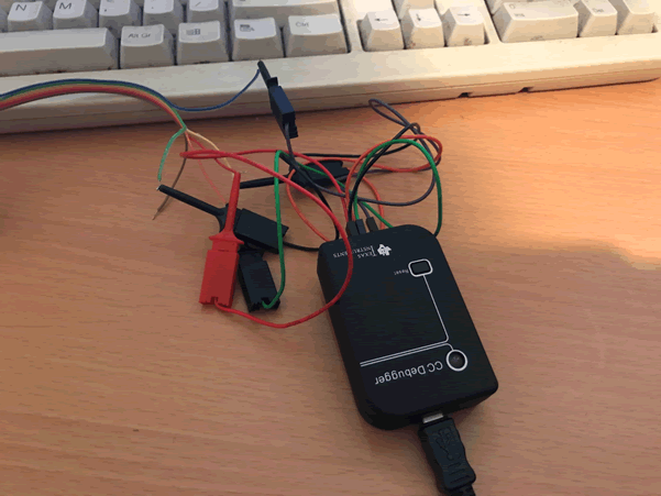
Yeah, they’re not the best grippers I had (I managed to misplace those), but don’t knock it, it worked. The unconnected brown wire goes to the NC pad.
If you have successfully connected all the pads, then the light on the CC Debugger will go green after the reset button is pressed.
The next step was to get hold of the software, and this caused a bit of a delay. To download the Texas Instruments software you need to register and validate your email address. For some reason, it takes six hours to send the validation email. I did this and had to wait overnight before I could download the software.
So, fresh in the morning I powered up my laptop, connected everything, turned it all on. Got a red light (because the Vdd connection had come unstuck, I shouldn’t have used cheap grippers), swore, reconnected everything again, got a green light and ran the software to read the firmware.
This is what I got:
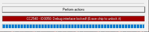
Ah, they’ve put security on the chip. Well that was a waste of time!
Fortunately we have had many devices that use CC2540s and don’t implement debug interface locking. We’ll blog about a couple of examples here shortly. Bear in mind that locking the interface isn’t always the end of it though…