In this blog we’re going to look at the process of dismantling and reverse engineering a hardware device to access JTAG ports. As a by-product, we’ll show you how the process results in some interesting artwork.
With hardware attacks, we often have several goals.
Firstly, we want to recover firmware from a device. This allows us to inspect operation of the device, find shared secrets, and often find vulnerabilities. In a perfect world, the firmware could be entirely open and not prove a security risk; we don’t yet live in a perfect IoT world!
Secondly, we want to obtain debug access to the device to help develop exploits. Buffer overflows are far easier to develop if you have GDB to show you the registers, memory and stack. Why can’t we use an emulator? Many embedded systems have tightly coupled hardware and software e.g. a DVR’s main executable may not run unless the video codec is connected and working.
Thirdly, devices often store sensitive data in RAM. This may be decrypted firmware, session keys, plaintext data from custom encryption algorithms and so on. Accessing this RAM often allows us to avoid reverse engineering and reimplementing aspects of the firmware.
To recover firmware, we can nearly always take the flash chips off the board and read them in a universal programmer. It is possible to encrypt external flash, but we don’t see this very often. Removing the chip and reading it takes time and effort though, and still leaves us without debug access.
JTAG will often allow us debug access, and hence access to RAM. It is possible to disable or secure JTAG, but nearly all devices we look at leave JTAG open. Frequently, the biggest barrier to us is finding the physical JTAG signals to connect to – TMS, TCK, TDI, TDO, TRST.
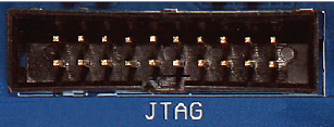
JTAG ports are often available on PCBs, left over from development, or used to program the device in the factory. A 2×5 or 2×10 header near the main processor or SoC is often a giveaway.
We find that physical JTAG ports are becoming less common on devices. I suspect this is for a few reasons. Manufacturers are opting to use serial bootloaders for loading firmware in the factory. This requires fewer signals, cheaper connectors, cheaper adaptors, and simpler software. Flash vendors can now program entire reels of chips with your firmware before mounting on the board.
Yet, even if the physical JTAG port is not present, the JTAG signals are still on the processor. And because the developers may never have used JTAG on the device, they may well have forgotten to secure it.
If the package is LQFP (or similar, with exposed pins), finding the signals can be as simple as looking up the pinout and clipping onto the chip. It’s far less simple with a 452-ball BGA package when there is no datasheet.
Sometimes you have no choice but to resort to reverse engineer the PCB, attempting to find JTAG.
We’re going to take you through some techniques we use to do this quickly and cheaply.
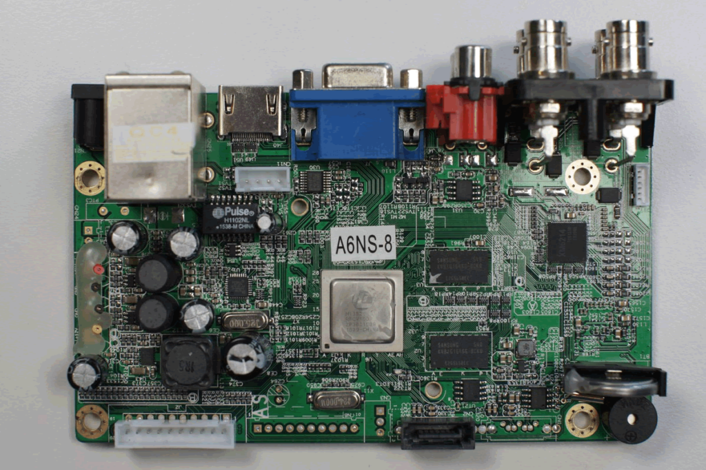
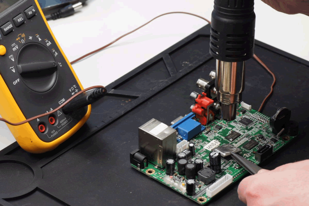
Our target device for this exercise is a QVIS DVR. It was vulnerable to Mirai; it ran XiongMai software running on a HiSilicon chipset. We didn’t actually need to disassemble this DVR board in order to extract the firmware – it’s in a 8-pin SOIC SPI flash on the back – but it’s a good example nonetheless.
The more sensitive components are removed using a hot air tool. 20 years ago, these cost £500 minimum. Nowadays, reasonable ones can be bought for £75. This has significantly lowered the barrier for reverse engineers.
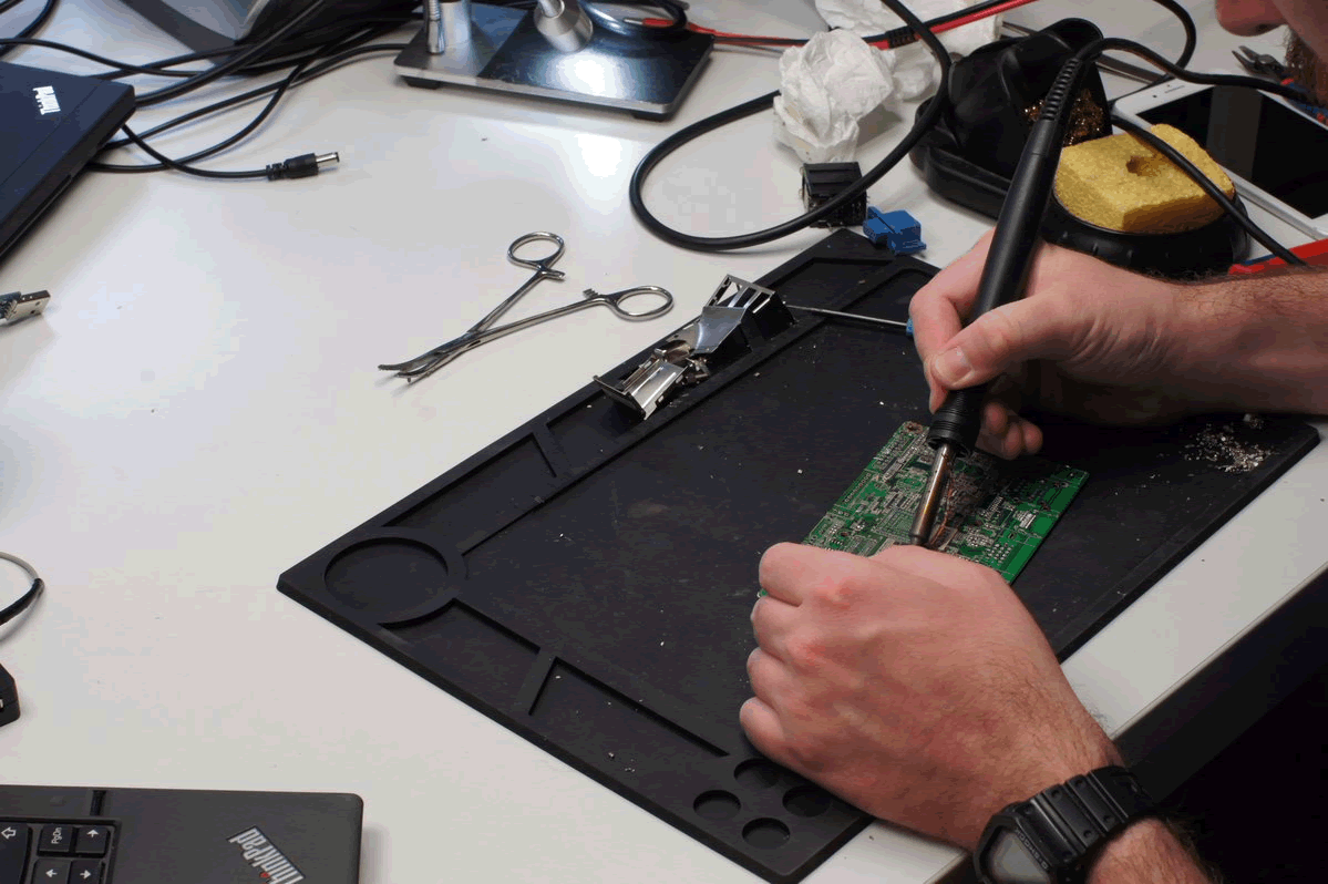
First, we preheat the areas we are working on with 200degC air. Then, we turn the hot air tool up to 400degC, and around 10s later the chip can be removed. Keep the tool moving.
Why do we preheat? It reduces thermal shock on components and means we minimise the amount of time components are exposed to very high temperatures.
Notice that we are using a thermocouple under the board to keep temperature in check, though you will quickly get a feel for this. You should practice this many times on worthless components before trying it on a device that has data you want on it!
Remember – generally we aren’t reworking a board to be put back into service. We don’t need to be nearly as rigorous as most rework technicians. A few melted plastic components are not an issue.
Less important components can be removed in a more aggressive manner. We heat the entire board up to melt all the solder, and then give it a few sharp taps on a block of wood – all the components fall off in one go!
This is a £30 toaster oven, which does the job just perfectly. We heat the board to around 230degC, just above the melting point of solder. We are less worried about damaging components at this stage. Don’t go much beyond this, or you risk damaging the PCB itself.
However, watch out for electrolytic capacitors exploding and other hot components. Heat and electronics can be very dangerous, so take precautions!
The board will have fair bit of solder spatter on it. We clean this up using flux and solder wick.
It doesn’t need to be perfect – just make sure nothing stands proud of the surface. There may be a few components left over – use the hot air tool to get rid of these.
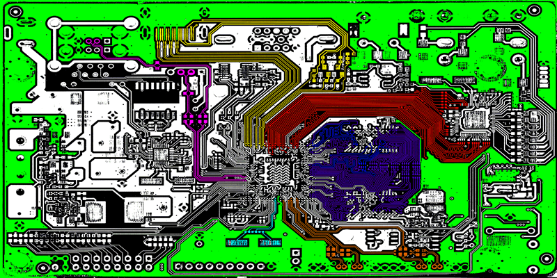
Now we’ve got the components and residue off, we can see the board much more clearly, particularly the traces and vias around the BGA packages.
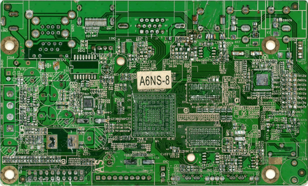
How did we get an image like that? A flatbed scanner. These are getting less and less easy to get hold of these days, especially ones that can deal with objects that are not perfectly flat. We use an Epson V600. Avoid the Canon LiDe scanners – these don’t work well at all.
Not only can we inspect the PCB itself, we can also inspect the HiSilicon BGA in more detail. The BGA package is called a “flip chip”. The small silicon die is mounted upside down in the middle of a carrier substrate. This is a miniature PCB, and the traces on this miniature PCB can give away the function of connected balls.
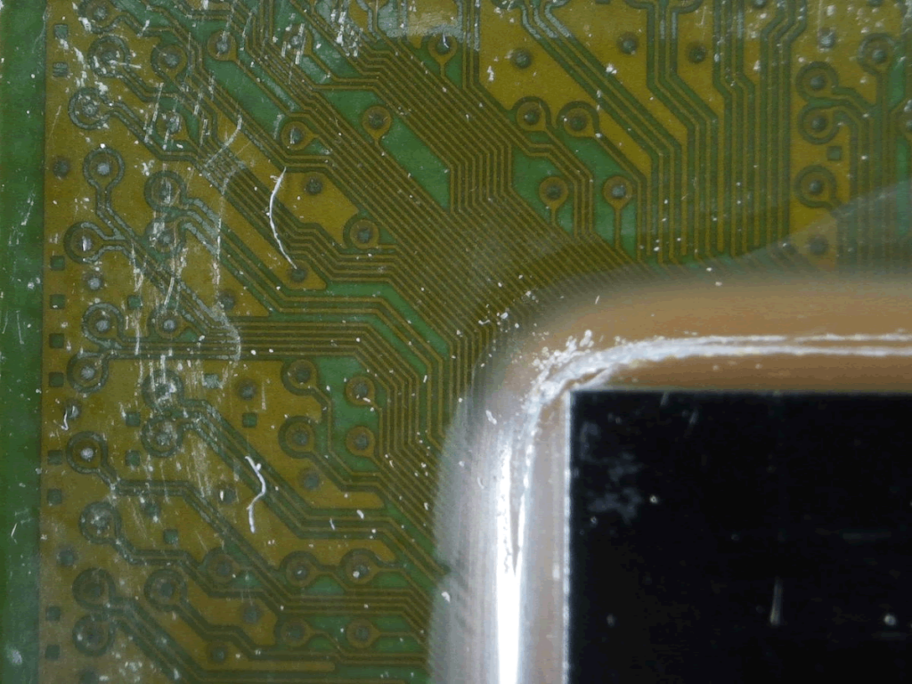
Back to the PCB – although the previous scan was helpful, we want clearer, more defined images. To do this, we remove the solder mask (the green lacquer) using wet and dry paper. Start relatively coarse and move to finer grades. Don’t go too far though – or you will remove the outer copper layer.
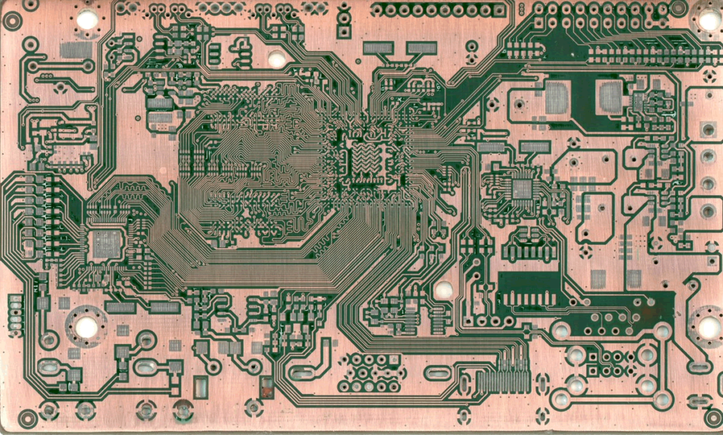
Getting a good image with the scanner can be challenging. Some are sensitive to the direction of sanding grain. A good clean with isopropyl alcohol also helps. Try to go for a good resolution – 1200 or 2400dpi seems to work well for 0.5mm pitch packages.
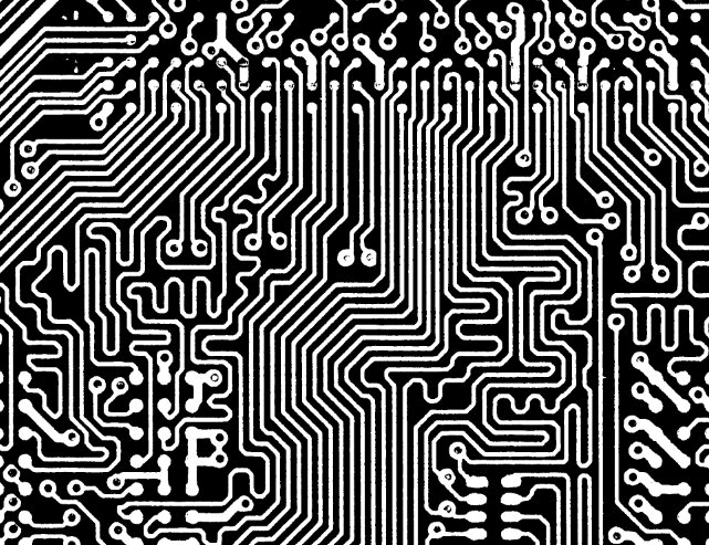
Import the image into an editor – we use paint.NET – and perform some post processing. Broadly this means changing to greyscale, adjusting levels to get good contrast, and then posterizing the image to black and white.
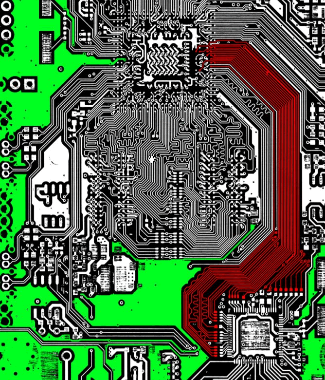
Now make some beautiful artwork: using paint.NET is it easy to use the paint bucket to fill areas of the board with colour. The ground plane becomes immediately obvious and following traces becomes easy – just click on one of the pads and the entire trace is filled in for you.
Then get your image printed out in large format and frame it for your kitchen wall as a talking point ?
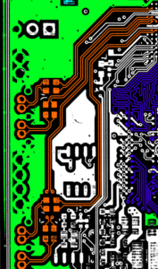
It’s also possible to infer function from how certain traces are formed.
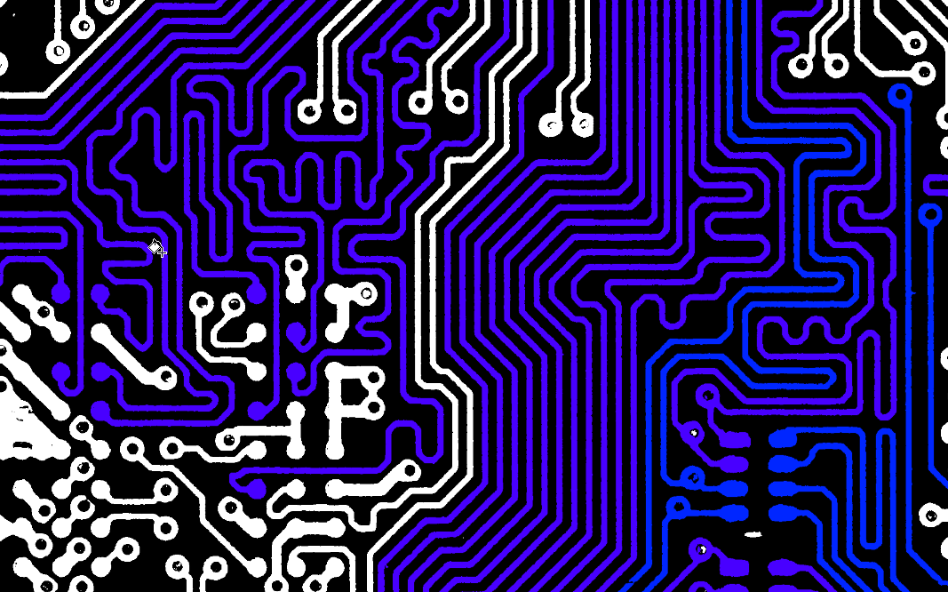
The squiggly blue lines are called “matched length traces”. These signify high-speed parallel interfaces, where it is essential that the signals across multiple traces arrive at the same time. These are common on SDRAM chips, but are also seen on display connections.
The orange lines closely following each other are differential pairs. These are used for high-speed serial connections – in this case SATA for the storage. The same is also seen for the USB interfaces.
To take this further, we can sand the other side of the PCB. The scanned image can be flipped and added as a layer behind the first.
This still leaves the inner layers of the board. You can keep on sanding and scanning through the entire board, but this takes a long time. Truth be told, most 4-layer boards do not contain much of interest in the inner layers. Move up to 8-layer and above, and that no longer holds true.