Over the last couple of weeks we have been debating the pros and cons of hardware obfuscation as a layer of defence.
After putting it out to the twittersphere, we were quite surprised at some of the responses it generated.
Obfuscation has a bad reputation, perhaps because too many web apps and cryptographic algorithms relied upon it in the past, in place of securely written code.
It does have a place in mobile apps (why wouldn’t you obfuscate your code, given it’s easy to do?) and we believe also in hardware.
This article is bound to generate some controversy, which we welcome as it will add to the debate.
Obfuscation has to come at a low cost for it to be worthwhile, otherwise one would be better off spending the money on even better security. Chipset choice (secure internal memory, a hardware RNG, adequate JTAG security, a cryptocoprocessor etc.), secure-by-design and a secure development lifecycle should be priorities. Obfuscation has to have minimal to zero additional cost for it to be worthwhile.
We also need to consider the motivation of the attacker. Are they focussed for example on a gaming console to enable pirated games to played? Are they financially motivated by profiting from hardware modding? Are they an inquisitive researcher, perhaps with malicious motivations to create a DDoS weapon, or maybe they have altruistic intentions of seeing security improve? The time each will spend on a device varies significantly.
There will always be a point where the effort expended does not justify the return, whatever the motivation.
So, the question is whether obfuscation can be used to increase the time required to reverse engineer a system to the point where the attacker will move on to another less secure device with a faster return?
It’s also a layer of protection in the event of the developers making mistakes. We have looked at several devices where JTAG or ICSP allows software readout, and the developers have replied “Oh, that was meant to be disabled”. If the JTAG or ICSP connector hadn’t have been immediately apparent, this would slow down an attacker.
Obfuscation is easy to introduce at the earliest stages of the design cycle and is easily validated. This is unlike many software controls (e.g. firmware signing) that are implemented later in projects and then left out due to lack of time.
What are you trying to protect?
Consumer IoT devices are unlikely to feature security that would resist a hardware reverse engineering expert or nation state grade attack for long. It would be reasonable for a consumer device to require say a day to a week of attention from someone with this level of expertise to recover something like a Wi-Fi PSK.
However, if you can slow the reverse engineering process down through obscurity, you raise the bar.
Easy wins for near-zero cost
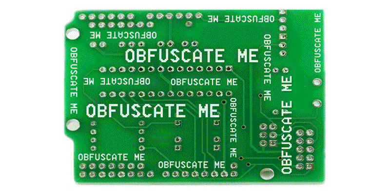
Remove the PCB silkscreen. Why mark up all your test points in production equipment?
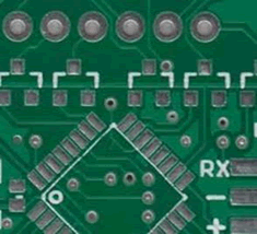
Hide your traces using the soldermask, the light green parts on this PCB. Again, why make the traces obvious?
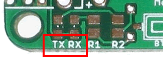
Remove test pads and debugging connections. Most consumer IoT product won’t have an expensive bill of materials. If it malfunctions and a firmware update won’t fix it, the manufacturer is unlikely to send a test engineer to debug and fix it; they’re going to send the customer a new product if in warranty. So why have debug interfaces enabled in production devices?
Ensuring that your schematics are not public. Request confidentiality from the FCC when filing your submissions.
Schematics will eventually leak into the public domain, but do what you can to limit that.
Set hardware and/or software fuses to prevent readout; bear in mind that both can be bypassed in some cases.
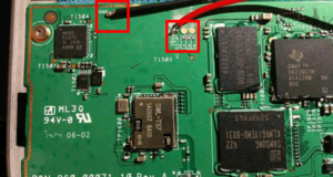
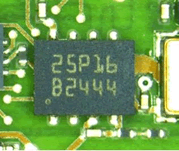
Remove all chipset markings – it’s a whole lot more difficult to identify a chip if there are no markings on them.
Ask your manufacturer to use tamper proof or one-way screws on the device casing. Not difficult to drill out, but only a more determined reverse engineer will bother.
Similarly, consider making the casing impossible to open without the attacker causing physical damage, using glue for example.
…yes, it’s easy to bypass, but an inquisitive device owner is less likely to trash their own device.
Minimal cost design considerations
Changing tack once you’re along the development phase can be costly, so these options only work at low cost if you consider them really early on.
Choose your chipset carefully. Ball Grid Array (BGA) package pins are hidden under the chip:
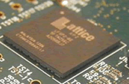
This means that it may have to be desoldered and reballed in order to identify the pinout. Great if you’re good at PCB rework, but it still slows down the attacker and reduces the number of people capable of attacking your device.
Consider physical anti tamper mechanisms on the device case. Yes, there’s almost always a method to bypass these, but it takes time.
More expensive options
There are various routes to take, such as camouflaging your chip, multi layer PCB design, buried and blind vias, tamper grids etc, but be careful not to spend money on obfuscation that should be spent on security.
WARNING
Hardware obfuscation does not provide security. It only works as an additional layer over and above good security practice. However, if you can make the reverse engineer’s life significantly harder for minimal cost, why wouldn’t you?
Useful resources
http://www.grandideastudio.com/wp-content/uploads/secure_embed_paper.pdf
http://ieeexplore.ieee.org/document/7820117/
http://www.engr.uconn.edu/~forte/Domenic_files/v2-acmsmall-combined_draft15_final_manuscript_4.pdf