TL:DR
Hardware security can be difficult to fathom, so I set out to research three password vaults as a newbie, sharing my findings.
I picked three popular hardware vaults, each with different components, requiring different skills and equipment.
Here’s how I learned about disassembly, chipset research, understanding pinouts, protocols and breaking encryption. I hope it’s useful!
Findings
Credentials in plaintext. In a password vault. Yes really.
Credentials that survive a hardware reset.
Reversible encryption.
And plenty more!
Introduction
I’m Phil (@Yekki_1), this is my first blog for PTP and my first hardware hacking project. I am lucky enough to be part of the PTP Academy which gives me the opportunities to discover different areas of infosec. Up front I’d like to thank the PTP hardware team (@tautology, @cybergibbons, and @iskuri1) who gave guidance and taught me some of the more technical details.
This series of blogs will go through the basics of hardware hacking, including the stages of a hardware test, identifying chips, continuity tests and ultimately reading data directly from the chips on the board. I will be doing these basics with 3 standalone password vaults, each with different chipsets and intricacies.
The three devices which were tested are:
RecZone Password Safe
- Identifying components and understanding datasheets
- Dumping SPI flash using a Raspberry Pi
- Reading the plain text data dump
PasswordFast
- Undertaking continuity test to confirm pinouts
- Investigating Microcontrollers
- Recognising encrypted data and realising the right time to stop
Full post here: Hacking Hardware Password Managers: passwordsFAST
Vault Password Keeper
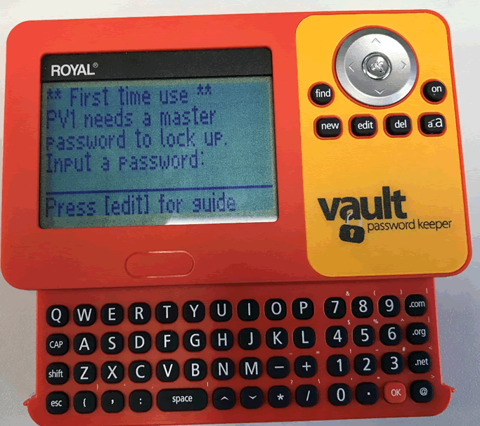
- Learning about CMOS flash and required hardware
- Fully destructive methods of removing chips from the board
- Using cryptoanalysis to decode stored data
Full post: Hacking Hardware Password Managers: Royal Vault Password Keeper
All these devices have a passcode to secure the device and the ability to add in the URL, username and password for each site. However one thing I did find consistent across all devices is the keyboard is hard to use and doesn’t encourage strong, complicated passwords.
Device set up
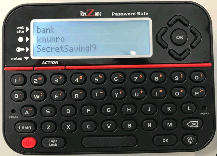
The first device is the RecZone Password Safe.

The first step of any hardware job is to add data onto the device, it’s important to add in a variety of data and can be beneficial to do lots of repeating letters and all possible characters, this will make it easier later on to identify the added data and helps with any decryption that might be required.
Once the data has been added, the next step is to get the case off and see what’s underneath. For this device there were 4 rubber feet under which were the screws that held the case together.
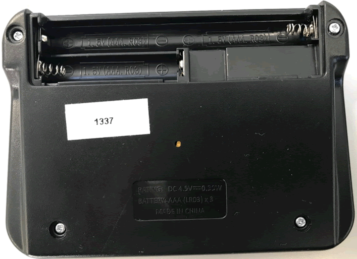
Removing the screws and getting the back off, the board becomes exposed and is a straightforward board.
Initial Inspection
The next step is a visual inspection of the board, working out what the board contains and which parts are of interest.
Starting with the back of the board:
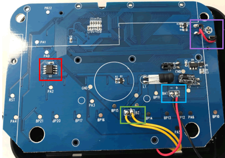
This is a basic board with only a few components, there are connections to other parts of the device, including the battery (blue square), screen backlight (purple square) and reset button (green square). The part I was most interested in was the 8pin flash chip in the red square.
The flash chip is normally the storage on a device, so this is where our passwords are likely to be stored.
Many chips can be identified by the text that appears on the top of them:
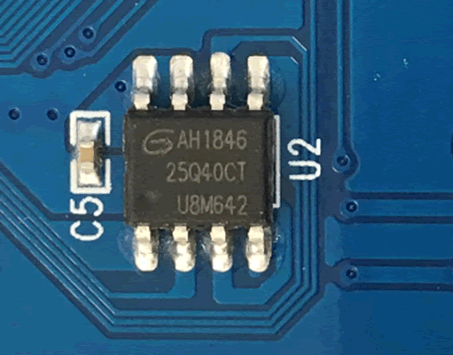
This chip is a 25Q40CT. Doing an internet search for this code, I was able to find the datasheet which will be needed after the initial inspection is finished.
What I wasn’t able to identify on the back of the board was a microcontroller, effectively the brains behind the device.
The top of the board was interesting as there were a lot of connections and what are known as “vias”, these provide a direct connection between the different layers of the board, this board only has 2 layers, so it’s a connection between the front and the back.
It is likely that these connect into something on the front of the board.
The front of the board has the keyboard connections. These types of connectors work by when the button is pressed, the metal circuit for each key is completed which sends a signal to the processor.
The backlight for the screen is connected by the wires on the right hand side, it is unlikely that all the vias on the back are for the screen.
Prising the screen off was possible with a bit of force, however it is very destructive and it turned out to be near impossible to properly reconnect it to re-use the device. It’s worth having spare devices when reverse engineering!
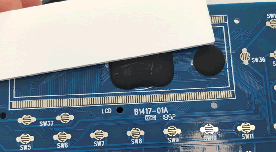
The screen was connected to the rails on the top and bottom allowing the display to work. A number of the vias however are used for the chip that was under the screen. This is a common thing nicknamed “blob on board”. It is done as a cost saving measure and although it can be removed, it’s dangerous with a high risk of damage to the chip.
For an introduction I decided that trying to remove the epoxy was out of scope. Instead I decided to focus on the flash memory.
Chipset
This is where the datasheet comes in handy. The chip is SPI flash, which is a common storage solution for small devices. The datasheet gives all the information about the chip, including which pin is for which function. This is critical to be able to read the data successfully.
The datasheet confirmed that the required voltage for the chip is 2.7~3.6V which means it was possible to power it up through a Raspberry Pi.
Continuity Testing
To confirm the information on the datasheet I undertook a continuity test. This test uses a multimeter to check connectivity between two pins. Simply set the multimeter to continuity mode:
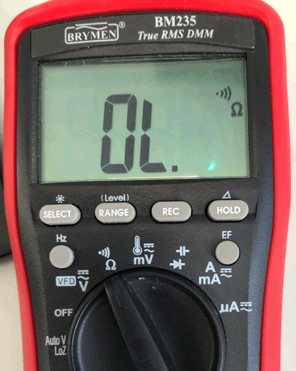
This mode beeps when a circuit is made. On the board there was a ground testing pin, so putting one probe on that and the other on pin 4 of the chip, a circuit should be completed.
The reading on the multimeter shows that a circuit was successfully created, therefore I was confident that I knew the pin layout for the chip.
Connecting it up
Using the datasheet the pinout can be compared against the raspberry pi SPI pins. The pins for the chip are:
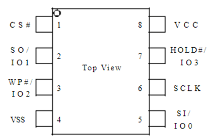
The names of the pins didn’t tie up with the raspberry pi pins, so I had to find out what each pin was:
- Vss – This is the main ground connection
- Vcc – This is the power for the chip
- CS# – Chip select – also known as slave select or (chip) enable it allows the selection of an integrated circuit out of several connected over the same bus. The chip on the board is the slave and what we read it from is the master.
- SO/IO1 – Data Output. This is the pin we will use the read the data from the chip.
- WP#/IO2 – Write protect input. Due to the fact we are reading, we might only have to write a single bit so this pin may not need to be connected.
- Hold#/IO3 – Hold input. Again, we are mostly reading, so this pin might not be needed.
- SCLK – This is the clock.
- SI/IO0 – Data Input. As we will need to write a bit before we can read, this will be required to allow that write function.
The SPI specific pins on the raspberry pi are:
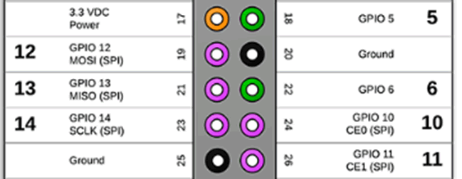
The key thing with SPI flash is that the MOSI (master output slave input) goes to SI (slave in) and MISO (master input slave output) goes to SO (slave out). The controller is the master and the flash chip is the slave. Normally when the chip is powered the MCU would be the master, however because I can connect and power the device through the chip, this lets the Pi interact with chip before the MCU can, resulting in the Pi becoming the master.
Connecting the PI and the chip results in this wiring: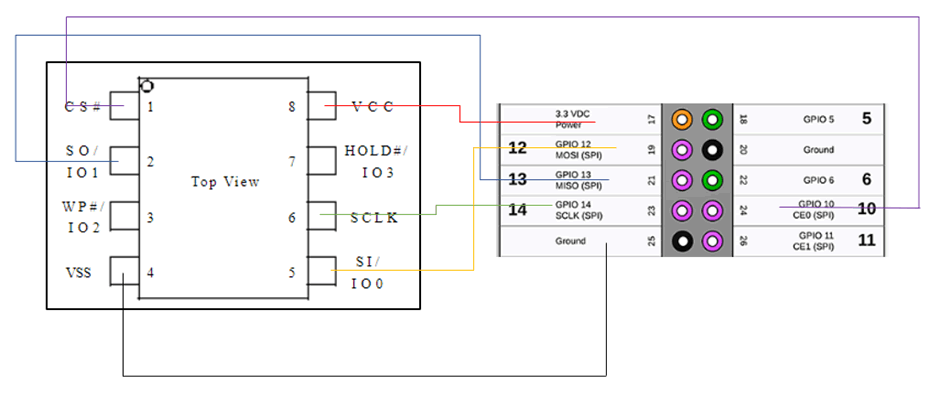
These connections allowed the chip to be powered without powering the rest of the board, the ground to be connected and the appropriate pins set up for reading the data.
I used a clip to connect up the chip. If you don’t have a clip it is possible to use grabbers to connect to each leg individually, however these make the entire process a lot more difficult.
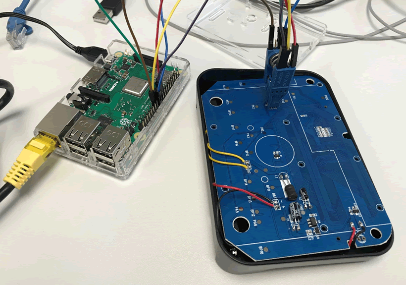
When connected, the pi was able to read the data. My pi was set up to have a static IP address and connected to a VM via a USB ethernet adapter allowing SSH access into the pi.
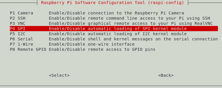
To read the data the pi needed the SPI interfaces enabled which is done via the raspi-config options
sudo raspi-config
Dumping the Data
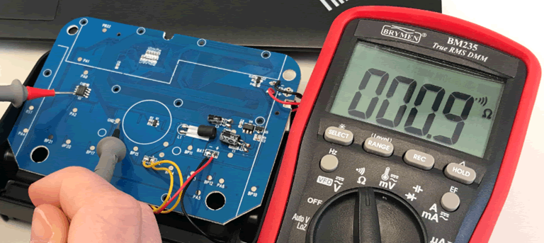
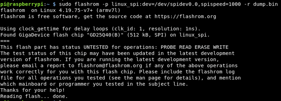
I was able to confirm that the chip was wired up properly using a program called flashrom:
sudo flashrom -p linux_spi:dev=/dev/spidev0.0,spispeed=1000
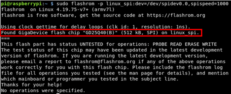
The program was able to detect the chip as a GigaDevice flash chip “DG25Q40(B)”. This meant that the chip was connected up properly and the data could be read off it.
To dump the data I appended the read flag and specified a file to output the data too.
sudo flashrom -p linux_spi:dev=/dev/spidev0.0,spispeed=1000 -r dump.bin
When the done message appeared, I knew that the data had been read. This however, wasn’t the end of the job.
Reading the data
The next step was to see what data was on the chip. To read the data I used a program called hexdump:
hexdump -C dump.bin
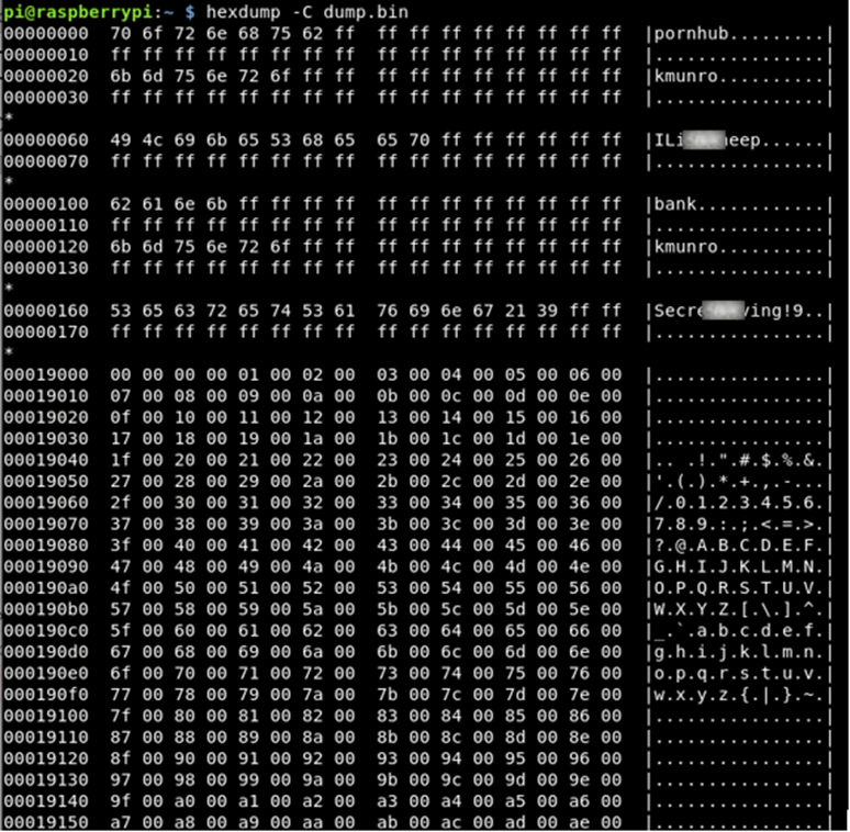
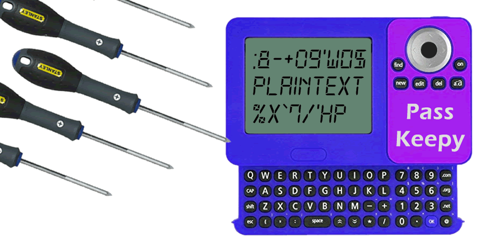
I could not believe it, the data was stored on the chip, in plain text! These are the details that I input into the device at the start of this process.
This data should be encrypted as an absolute minimum for this… But it gets worse, I used the reset on the device and was asked to set a new master pin (as I had to at the very first bootup). I then re-dumped the chip:
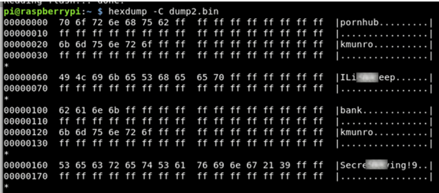
The data was still there!
What this means is if a user presses the reset button and sells the device, all of their passwords can still be read in plain text directly off the chip.
That is absolutely nuts!
On the second dump of the data I also found this:
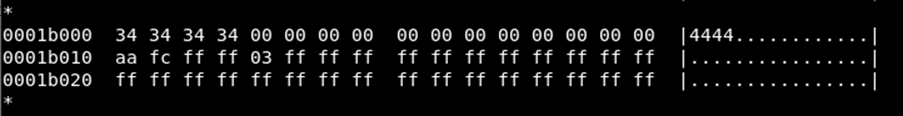
This is the master 4 digit pin that I set after the reset. Again in plain text!
Someone using a device like this, hopefully wouldn’t have password reuse, but it’s not out of the realms of possibility, especially if it’s a 4 digit code similar to things like, their phone pin, or their bank card.
There might have been a software based reset, rather than the hardware reset button which I would have liked to have tested but unfortunately I removed the screen too early which turned out to be fully destructive. This was a very valuable lesson I learnt about starting with the least destructive methods and only moving to most destructive once all other avenues have been looked at.
We reached out to the manufacturer of the device to inform them of this security vulnerability, however we did not receive any acknowledgement back from them.
This has been a very interesting first look into hardware hacking, I have learnt a lot from this device, including the process and the importance of not doing fully destructive testing until all other tests have been completed.
It did make me wonder though, what could they have done differently and have the other devices secured the data better?
Part 2 of this series will look at the PasswordFast device and will show an almost entirely different set of hardware to do a very similar job.
For reference here are the links to all three hacking hardware password manager posts:
https://www.pentestpartners.com/security-blog/hacking-hardware-password-managers-the-reczone/
https://www.pentestpartners.com/security-blog/hacking-hardware-password-managers-passwordsfast/
https://www.pentestpartners.com/security-blog/hacking-hardware-password-managers-royal-vault-password-keeper/