This second post is a companion to the DEF CON 29 video. Starts at 25:43 here.
About a year ago I did some research into adding new capabilities to Samsung’s NFC chips in their smartphones, by bypassing their signature protection and applying code patches. This allowed me to add custom NFC tag capabilities to Samsung phones, however it was limited solely to smartphones manufactured by Samsung and even then, this was country dependant. Due to this, in 2020, I decided to try and tackle the biggest manufacturer of NFC technologies in the world: NXP, and their PN series, which is used by pretty much every smartphone manufacturer.
It can’t be understated just how many phones use this chip series, if your phone has NFC capabilities, it’s probably using one of these, even if it’s an iPhone, there’s a high likelihood that you are holding a phone with one of these chips in your hand right now.
Because of this, I felt that finding a signature bypass vulnerability in this chip would allow a user, with root access and sufficient reverse-engineering skills, to replicate my original project and add additional capabilities to this chip.
PN553
My initial chip of choice was the NXP PN553, as the test phone I had immediately available and rooted used this for all of its NFC functionality. This chip, and pretty much every chip in this series, had almost no documentation available beyond some datasheets containing specifications about their capabilities and some limited information about their architecture. However, there was some information that I could garner from this, and from looking at the content of my phone’s filesystem:
- The chips were mainly used in mobile devices, but some chips were available on development boards for embedded projects
- Used an ARM Cortex-M architecture, a standard architecture which uses Thumb-mode operations.
- Multiple chips in the series: including the PN547, PN548, PN551 and PN5180, all of which used a similar firmware update mechanism.
I also found that there were older chips in the series, such as the PN544, which were different, using an 8051-based architecture. I decided not to look into these too much as they were not used in any modern phones.
The similarities between protocols and firmware updates between the modern chipsets were clear, due to the fact that my phone contained firmware update blobs for each of these chips, and used logging strings referenced as “PN54X” no matter what chip was in use.
Communication
When reverse-engineering a piece of peripheral hardware on a phone, there are some great shortcuts which can be used to analyse the communication between the core Operating System and the chip.
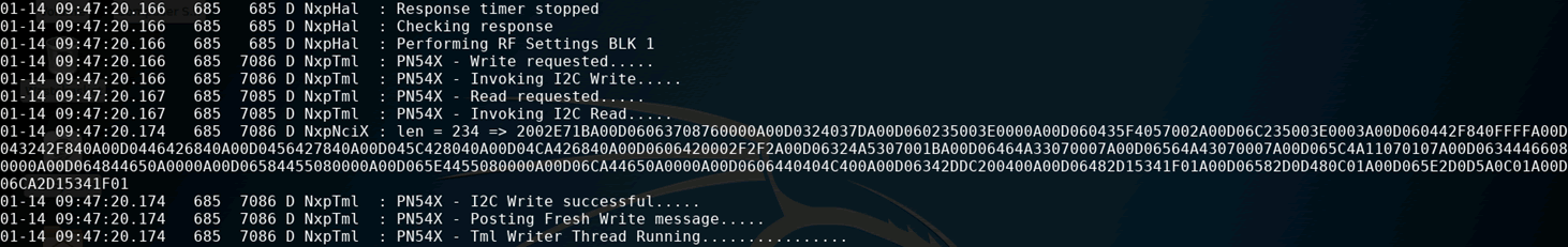
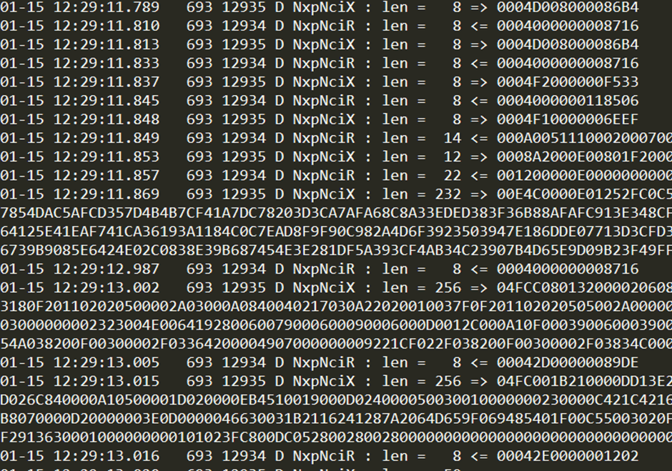
The first method, if you are lucky, is to use adb logcat. This will dump the Android system log, which occasionally contains verbose information regarding how system services are functioning. In this case, it provided me with the full payloads being sent and received to the chip via its I2C interface.
Also, using a statically compiled version of the strace tool, which can easily be found online, one can hook into the NFC services of the phone, and dump all system calls, including those to device files. This provides a deep insight into the exact reads, writes and IOCTLs in use. IOCTLs are system calls made to files in Linux which alter configurations, but don’t serve to read or write data, and are very commonly used with files located in the /dev/ directory.
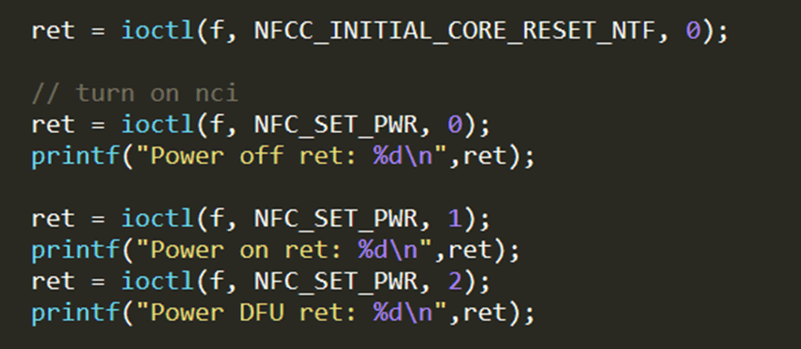
The strace tool can be beneficial in identifying which device files are being written to. In this instance I used it to identify which I2C interface was being used to communicate with the chip. I found that, instead of using files references as /dev/i2c*, it was instead using a custom driver which facilitated both I2C communication and GPIO power controls, which presented itself as /dev/nq-nci.
If I wanted to communicate with the chip, all I would need to do is access this device file, with all NFC functionality on the phone turned off. Accessing this wouldn’t be possible when the NFC functionality is enabled, as the file is already in use by the Android framework.
Firmware Updates
Looking at the standard communication that was performed on the chip, I found that it was using NCI for all NFC connectivity. This is a standard protocol which doesn’t contain a large amount of scope for exploitation due to its rigid standards. I decided to attack the bootloader, which would likely be using a custom protocol. I didn’t know anything about this protocol, so I needed to find a way to force firmware updates.
I noted that in the filesystem there were both “firmware” and “recovery” binary blobs for the chip, stored in the /vendor partition:
- libpn553_fw.so
- libpn553_rec.so
As I was root on the phone, I had mounted the /vendor partition as writeable. I then decided to swap these two filenames and restart the NFC service on the phone, which could be performed using the standard menu in the Android shell. This made the phone verify the version number of the current firmware against the one in the file, and if they differed it performed the firmware update. This allowed me to reverse-engineer this process.
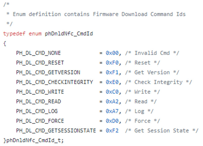
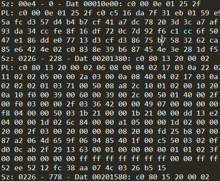
The protocol was found to be unique to NXP chips, and each packet was constructed as follows:
| Byte | 0 | 1 | 2 | 3 … x | x+1 | x+2 |
| Use | Status | Size | Command | Parameters | CRC-16 | |
These commands were encapsulated in 0xfc byte chunks, meaning that larger commands were sent in stages. I found that some parts of the NXP source code for the Android drivers were available, which allowed me to assess the commands that were being sent for the update.
As I now had a good trace of how the updates were performed, I decided to develop a simple update tool of my own, which I could then use to try and break the process later. Using a combination of logcat and strace I found that the chip would switch to firmware update mode by sending a specific IOCTL. Using the open-source headers in the Linux kernel, I could get the correct addresses and perform these IOCTLs.
While I could just replay the update commands I had retrieved from logcat, I wanted to see exactly how the firmware updates were formatted. I took the file “libpn553_fw.so” and chucked it in a hex editor. I was expecting this to be a shared library, due to the “.so” extension, however its contents weren’t quite what I was expecting. Analysis of the file found that it contained no directly executable code, but that it contained a huge block of unusually formatted data.
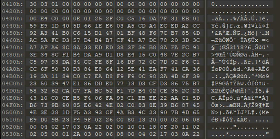
A brief comparison between this and the initial firmware update commands retrieved via logcat quickly revealed that this was the sequence of firmware update commands. It was sequenced as two bytes which defined the size of the command, and then the command itself, in an unencapsulated format. This allowed me to extract all of the commands (which were all C0 Write commands) and get some cursory information around their contents.
Except for the first, each packet had three bytes to specify a memory address, two bytes for a size, and then the payload itself. There was also 32 bytes of high entropy data at the end of each command, which I presumed was some kind of hash used to perform integrity checks upon the update.
I used this update file to stitch together what the firmware would look like in memory. I noted that the code was very small and contained multiple references to executed memory, which was at lower addresses in memory, implying that there were standard libraries baked into the bootloader which could be referenced from the firmware.
While I could now perform firmware updates, and learned a few further details about them, such as the fact that the update sequence could not be changed and skipping any blocks would break the update, I did not yet have a full understanding of how this functioned. I decided to move on from this temporarily to understand other key aspects of the chip.
Command Enumeration
I wanted to see if there were any undocumented commands. To this end, I wrote a tool which would constantly power cycle the chip while sending commands from 0x00 to 0xff, and check the error responses at different sizes. This revealed command 0xF4, which returned the chip ID, but nothing else of interest. I also found that commands 0x80 and 0x83 would place the chip in an unknown state. I didn’t pursue these much further.
I decided to assess the capabilities of the commands that were documented, to see if they could reveal anything interesting. The first thing I noted was that there were two commands which could read some memory.
The command 0xA2 allowed the reading back of any memory location which was also writable by firmware updates. This meant that I could dump the memory I already had access to, but not read any arbitrary memory.
The command 0xE0, which was defined as a “check integrity” command, provided checksums of memory, but also took a four-byte address, which would return four bytes of data which I presumed to be part of the device configuration.

I noted that incrementing the value by one would shift the data by four bytes, implying that there was a lot more than four bytes of data available. Stitching the memory returned from this, using incrementing values, allowed me to generate a 0xf00 byte block of data, which contained some unknown data, and some which was easy to identify.
I found a block of data which was 0xc0 bytes in size, followed by a value of 0x10001. This pattern was consistent with an RSA public key, and was likely to be the key used as part of the firmware update protection, which would allow me to learn more about how updates were performed, because I would be able to more easily spot a signature in the update payload.
There was an additional write command, 0xA7, which allowed for logging of 64 bytes of data into the configuration memory. This had no bearing on the functionality of the device, however, and seemed to purely be used for logging.
Bricking The Chip
Having learned about the firmware update process, I decided to have a further look at the core NCI functionality, available in the firmware for enabling NFC capabilities. I knew, from previous research, that there were two key areas where this chip may contain vulnerabilities. NCI allows for custom, vendor-only commands to be added, and also allows for custom configurations to be implemented. While I didn’t find any unusual vendor commands, I did find a huge number of configurations, which I decided to fuzz, using the NCI Config Write command, and incrementing bitwise XORs over each bit of each configuration. I did this as it was highly likely that each bit would correspond to some part of the configuration, or at the very least cause an interesting crash.
This resulted in the firmware crashing, and being rendered inoperable. I found that I could no longer execute NCI commands, or boot into the firmware, however I could still access the bootloader firmware update process. Performing a clean update did not repair the chip.
Looking into this further, and using the identified configuration read command, I noted that I had written values over some configurations, that were likely to be the cause of the chip being bricked.
These configurations could not be modified because I did not have any write access to this area of memory, however there was a high likelihood that a modified firmware update could repair it, and bring the chip back to life. As such, I decided to persevere with trying to break the firmware update protections.
Firmware Update Sequence
Using the information I had gathered from the firmware update commands, I assumed that the first write command sent, which contained 0xe0 bytes of high entropy data, and a version number, contained the firmware update’s signature, and a 32-byte hash. It took a long time to work out, trying different potential hashing algorithms and methodologies, but I eventually worked out that the chip was using a hash-chain approach.
Essentially, the first written block contained a SHA-256 hash of the next block in the sequence, which also contained a SHA-256 hash. The next block would do the same, cascading throughout the entire process, with the only block which didn’t contain a hash being the last one (this’ll become important later).
This process was interesting, because it maintained the integrity of the firmware, while only needing to verify a signature over the first hash. This would prevent an attacker from even being able to write an unsigned block to memory.
Breaking The Sequence
Despite this update sequence being interesting, and on the surface secure, it added complexity which could cause there to be exploitable weaknesses. I noted that the last block in the sequence, which had no hash, could be written multiple times without receiving any errors. Due to this, I assumed that the firmware update was using global memory which could potentially be overwritten by erroneous commands.
I decided to send a command, which wasn’t a firmware write, but was the size of a firmware update command, including the hash, before the final, hash-less block was sent.
While this command received an error response, because it was too large, it also prevented the last block from being written, meaning that I had likely overwritten the next hash in the sequence in memory. I tried to push this further, by generating a hash for a slightly modified version of the last block, and then sending that modified version. This was found to be effective, meaning that I could now write arbitrary memory!
In order to fully prove that this was effective, I decided to un-brick the chip. I had a backup of the working configuration from when I started the project. I generated a block that would overwrite the broken configuration with the working one.
This was found to be effective, and I could once again access the core firmware. I wanted to prove that I could push this to full code execution, by implementing a simple feature: arbitrary memory reads, with the goal of dumping the bootloader.
Exploiting The Vulnerability
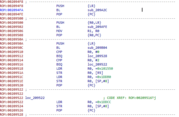
I found that almost all NCI commands were accessed in the inaccessible part of memory. Some complex tables at the start of the firmware were actually used to reference these for the firmware, so that they could be altered to work from the firmware update if needed. Unfortunately, these tables accessed memory I didn’t know about and they looked like messing with them could do some real damage. Due to this, I decided to focus on a command that I knew would change between updates: the “firmware version” read NCI command.
I searched for the bytes that represented the version number and found them embedded in the binary. These were referenced by a single function, that pointed to them and then called a second function. As the version number was the second argument in the function, I assumed this would be a memcpy for responses to the read command.
I used my new arbitrary memory write to overwrite this block, so that the “BL” function call pointed to empty memory which I could use to create a new function. Using C and the gcc “-c” flag, I generated raw machine code which can then be patched in for this purpose, and I could use this to alter this function to write different memory to the pointer in the first argument.
I started with an empty function call, this was shown to send an empty response to the firmware version command, which supported the theory that the function was likely to be a memcpy.
I now had control over the data returned, but not the parameters being sent via NCI. To exploit this, I modified my code to search the entirety of RAM for a unique value. I sent an NCI firmware read command with the parameters “FA CE FA CE”, and then modified my C code to search for this in RAM, which I deduced would start at 0x100000 in memory, as lots of writes were noted in the firmware to this memory space. I would then make my code return the exact pointer where it found my unique value. This found that the command pointer was stored at 0x100007, meaning I could use this parameter to request arbitrary memory pointers and return the data.
As I could now read arbitrary memory, I decided to write a sequence that would dump the entirety of the bootloader, the entirety of RAM, and the entirety of the firmware memory space. This was achieved by constantly power-cycling and sending incrementing values. Reverse engineering this data would give me a full understanding of the entirety of the chip’s functionality, and allow me to alter anything I wanted.
I could have extended this functionality further, to modify its NFC functionality, however at this stage I decided to stop here and start disclosure.
PN5180
During the disclosure, I had a look at the PN5180. This is an outlier in the chip series as it is mainly used for embedded electronics projects unrelated to smartphones. Originally, I believed it was only used for hobbyist electronics projects, but I recently learned that it is designed and advertised as a chip used in Point-of-Sale systems!
Development boards and libraries are widely available for this chip, so I bought one and hooked the relevant pins up to a Raspberry Pi.
This chip used an SPI interface, rather than I2C, and I had to connect the GPIO pins and do a bit of reading about how each one worked. I was happy to note that the firmware update sequence was almost exactly the same as the PN553’s, with the only caveat being an additional byte at the start of all sent payloads, which was easy to add. Firmware updates were provided in libraries as structures of byte arrays, rather than “.so” files.
I quickly confirmed that the same signature-bypass technique was applicable, and that I could modify arbitrary code, however I found that the core firmware no longer used NCI, and instead used a custom protocol which was much simpler and documented in the publicly available libraries.
As part of this protocol, there was a command that allowed reading from a specific address in the EEPROM. I found its pointer in the firmware, and realised that I could manipulate this, rather than use drastic code changes, to dump this device’s bootloader as well.
This would take a few hours, but would be quicker to develop and give me direct access to the contents of this chip.
This demonstrated that the signature bypass would be applicable to almost all PN-series chips.
SN100
Special mention should be given to the NXP SN series. During my research I stumbled on this chip in more modern smartphones and decided to try and attack it as well. I quickly noted that, while the firmware update commands were superficially similar, the signature bypass no longer worked. This was due to the fact that the chip’s bootloader had been modified to allow for encryption as well as signing, and meant that I could no longer just modify the hash as needed. I put a concerted effort into trying to break this process. I never managed to bypass the protections on this latest iteration of NXP’s product.
Disclosure
As this vulnerability affected an entire chip series, with incredibly diverse use-cases, I decided that it would be necessary to disclose my findings directly to NXP. NXP make it very simple to perform this disclosure, with a publicly available PSIRT page which can be found with a simple Google search.
I disclosed the vulnerability, with a PoC for the PN553 to NXP in June 2020, and they swiftly confirmed that it was valid, providing information about what would happen next and how they were going to move forward. During this process, they requested an extended disclosure period of 14 months, bringing the public release date to August 2021. I accepted this, due to a few extremely important factors.
In order to remediate this vulnerability, NXP would need to patch the first-stage bootloader of every chip, for every firmware version, essentially meaning that they would be overwriting the code that was necessary for the chips to even start. If this process was performed incorrectly, a huge number of NFC chips would be rendered completely unusable, with no way of repairing them. Discussion with NXP outlined that this would be performed in phased rollouts, meaning that the process could be controlled, and this was performed within this disclosure period.
Conclusion
This signature bypass is only useful on phones for adding new, interesting functionality to the NFC chips. Its existence on the PN5180 means that it could be used to expand the functionality of hobbyist projects as well. There is small scope for this weakness to be used in supply-chain attacks on NFC-based PoS devices, however this would be very limited compared to what could be done with the rest of the hardware. It may not be weaponizable on other people’s hardware, but it certainly can make your phone more powerful.